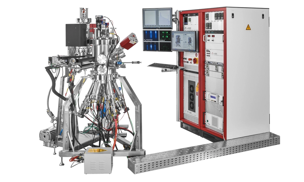
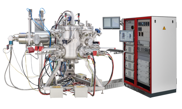
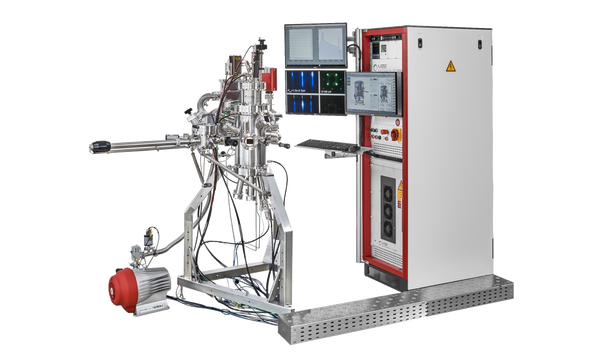
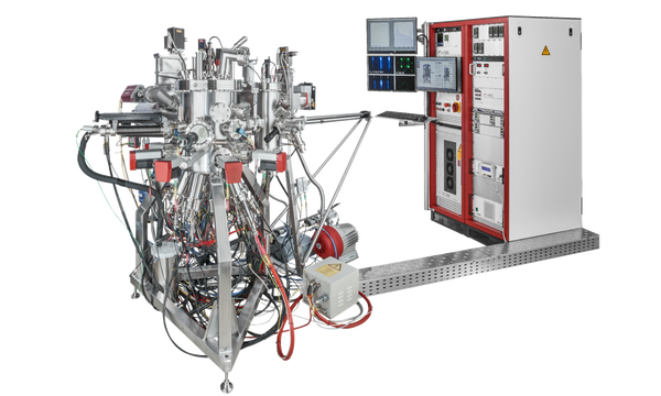
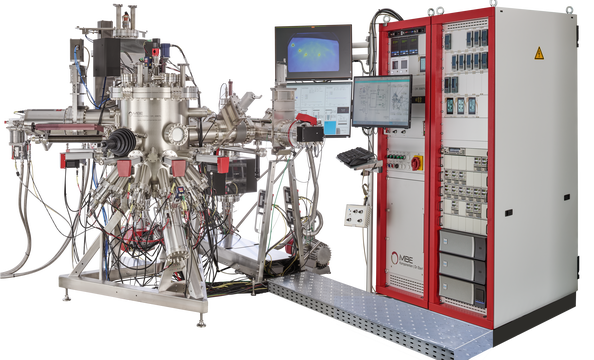
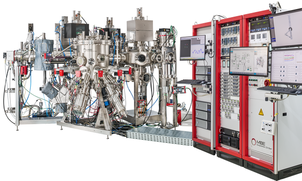
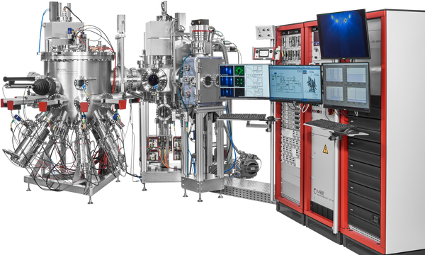
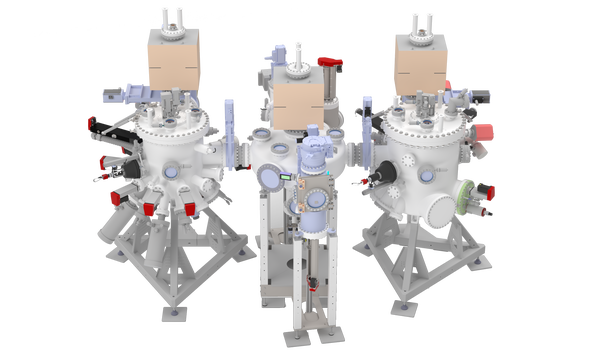
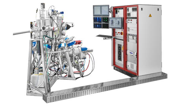
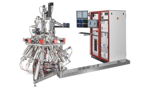
Mini III/V, II/VI, topological insulator or other material MBE system
- Compact and versatile research MBE system with small footprint
- Applications: II-VI, III-V, IV-IV, metals, magnetic materials, topological insulators, nanowire growth, oxides, organic materials
- 9 source ports DN40CF (O.D. 2.75’’) or 8 source ports (2x DN63CF (O.D. 4.5’’), 6x DN40CF (O.D. 2.75’’))
- Wide range of source options
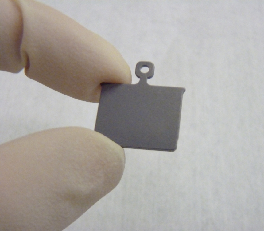
- Sample size : flag style 10x10 mm2 , 1’’ or 2’’ wafer
- Effective UHV pumping system
- Stainless steel LN2 cooling shroud
- Low energy and LN2 consumption
- In-situ monitoring capability
- Professional support by PhD MBE experts
General Information
The OCTOPLUS 300 system is ideally suited for material deposition on small samples. It provides good access and easy operation and maintenance. The chamber design of the OCTOPLUS 300 plus various state-of-the-art components allow layer by layer precise MBE growth.
Outstanding features of the OCTOPLUS 300 are the high reliability and versatility of the system and its small footprint. These features make the OCTOPLUS 300 system particularly suited for applications in research and development. Nonetheless specific production processes are also covered.
The standard version of the OCTOPLUS 300 comprises 8 source ports, two ports with 4.5 inch (DN63CF) and six ports with 2.75 inch (DN40CF) flange size. By using Source Clusters up to 10 sources can be integrated into the system. A rapid pump-down load lock chamber with a horizontally working transfer-rod system allows the user an easy substrate introduction without breaking the vacuum of the MBE chamber.
We provide different kinds of effusion cells, valved cracker sources, gas sources and substrate manipulators according to all our customers’ requirements. A well-manageable in-situ characterization is obtained by using beam-flux-gauges, pyrometers, RHEED systems or quadrupole mass analyzers (QMA).
We are happy to discuss your MBE system specifications and give competent advice for your application. Do not hesitate to contact us.
Options for OCTOPLUS 300
- Additional load lock or buffer chambers
- Wafer transfer system
- 2 cm³, 10 cm³, 35 cm³, 60 cm³ effusion cells, source clusters, electron beam evaporators, cracker and valved cracker sources, manipulators, power supplies and control units
- Pumping system (ion getter pumps, turbopumps, cryopumps etc.)
- Control system
- In-situ characterization tools, e.g. ion gauge, Quartz Crystal Microbalance (QCM), pyrometer, RHEED, QMA
Technical Characteristics
| Size of deposition chamber | 300 mm I.D. |
| Base pressure | < 5x10-11 mbar |
| Pumping | turbopump, ion getter pump and TSP |
| Cooling Shroud | LN2 or water cooling |
| Substrate heater temperature | up to 1200°C |
| Substate size | small sample plates or up to 2" wafers |
| Bakeout temperature | up to 200°C |
| Source ports | 9 ports DN40CF or 8 ports (2xDN63CF, 6xDN40CF) |
| Source types | effusion cells, e-beam evaporators, sublimation sources, valved cracker sources, gas sources |
| Shutters | soft-acting rotary shutters |
| In-situ monitoring | ion gauge, QCM, pyrometer, RHEED, QMA |
| Sample transfer | linear transfer rod (manual) |
| Load lock | magazine with 6 substrates turbo-pumped |
| Control software | Tiny Tusker |
| Service | system installation and acceptance testing |
Examples for applications and corresponding sources
| Material System | Effusion Cells | Sublimation Sources | Valved / Cracker Sources | Plasma Sources | E-Beam evaporators |
|---|---|---|---|---|---|
| Products | WEZ NTEZ OME HTEZ | SUKO SUSI HTS DECO | VACS VGCS VCS VSCS | FMP RFP | EBVV |
| III/V | Ga, In, Al | C, Si doping | As, P, Sb | ||
| II/VI | Zn, Cd, Be | S, Se, Te | N-doping | ||
| IV | Ge, Sn, Pb | B, P, Sb doping | Si, Ge | ||
| GaN | Ga, In, Al | N | |||
| Metals | Cu, Al, Ni, Co, Pb... | Pt, Ta, Pd, Mo, W | |||
| Topological Insulators Thermoelectrics | Ge, Sn, Te, Bi, GeSb | Se, Te, Sb, alkali metals | B | ||
| Graphene / Silicene | C, Si | ||||
| Oxides | Fe, Ni, Mn, Bi, Eu,Ga, … | O | |||
| Thin Film Solar Cells | Cu, Ga, In, Zn, NaF,Fe, Sn | S, Se |
Trusted expertise since 1990
Based on many years of active research experience in the field of growth and doping applications our team develops and manufactures the OCTOPLUS 300 and all essential components. Each product is assembled and carefully tested in-house. We are happy to discuss your MBE system specifications and give competent advice for your application.
The OCTOPLUS 300 is in use in leading laboratories. On demand we transmit a detailed list of references. Please contact our sales department for further questions and specification information.
Technical specifications are subject to change without notice.
