- 1020 /cm3 n-type doping in Si/SiGe MBE
- P-doping through GaP decomposition
- High P incorporation rate
- Minimum memory effects
- Easy to install and to operate
- Sharp doping profiles
- Precise and fast flux control
Introduction
The Phosphorus Doping Source DECO-D is an ultra pure source for P 2 , based on the decomposition of GaP. At typical operation temperatures of about 600°C - 700°C GaP is essentially decomposed to Ga and P2 . Additional cracking is not necessary and the accumulation of P4 (White Phosphorus) is reduced to a minimum.


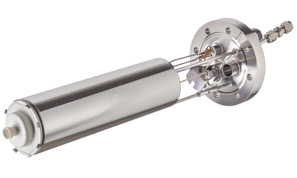
The simple construction of the DECO-D, based on our WEZ and PEZ effusion cells, and the specially designed Ga-Trapping-Cap System have the advantages of easy mounting, full compatibility to all MBE systems, high reliability and low cost. The operation of the DECO-D is comparable to usual effusion cells and does not require complicated mechanical valves and controllers. MBE-Komponenten GmbH has developed special sources based on the Ga-Trapping-Cap System. We build the DECO-D optimized for special doping applications, e.g. as phosphorus doping cell for Si MBE with a reduced cell shutdown time.
The heater of the DECO-D is designed very similarly to the WEZ-heater which consists of a Ta wire filament supported by PBN rings. Crucible material is PBN. With this design minimum outgassing at operation temperature is achieved, in combination with excellent reliability, long-term stability and extended lifetime.
Excellent operation temperature stability of ±0.1°K is achieved by an improved design of the thermocouple assembly. This assembly touches the crucible near the base. The direct touch technique and the use of double pairs of TC-alloy wires ensure a reproducible and stable measurement of the real crucible temperature.
Ga-Trapping Cap Unit
The DECO source features a unique Ga-Trapping Cap Unit system that provides a very pure P2 beam by decomposition of GaP. The idea underlying that unit is the sublimation of phosphorus from GaP at rather moderate temperatures at which gallium has only a negligible vapor pressure. By special baffle plates parasitic Ga atoms are efficiently separated from the P2 beam, thus producing a very pure P2 flux.
The Ga-Trapping Cap Unit is a simple but effective design consisting of only a small number of well-designed parts which are mounted onto the PBN crucible without additional tools or holders. For source maintenance and crucible refilling the unit is likewise easily removable.
Upon special request, a complete Ga-Trapping-Cap Unit is available as a
product of its own, for retrofitting standard effusion cells.
Inquire for further information on compatibility.
operating temperatures 900-1200°C for growth applications
precise adjustment of P2 incorporation into GaAsP. GalnAsP, etc., compound layers
P2:P4 ratio about 150:1
very low parasitic Ga flux (P:Ga > 105)
(P:Ga > 103 without Ga-Trapping Cap Unit)high efficiency : about 20 g P in GaP for 100µm film thickness
marginal white phosphorus accumulation in MBE system
no additional safety facilities needed in contrast to PH3 , AsH3 or valved elemental phosporus crackers
no bakeout necessary before opening the system
compatible with standard III/V solid source MBE
Application
Typical applications of our DECO-D phosporus doping source are high level and sharp delta-doping with Phosphorus in Si/SiGe MBE. Small crucible charges, large double layer shutters, integrated water cooling and reduced shielding allow a fast shutdown of the cell after the doping. High 10 20 /cm 3 doping and sharp delta-doping have been reported in literature applying the DECO-D from MBE-Komponenten GmbH. Due to its small dimensions and easy operation the DECO-D is ideally suited for all types of MBE systems.
Single crystal GaP material with a purity >6N is recommended as source material.
The DECO-D has been successfully operated in many MBE laboratories worldwide. The following three figures demonstrate the unique performance of devices fabricated by means of the DECO-D.
The figure below shows a sharp P-doping profile in a Si layer with two P-delta-layers. The experiment was performed at the Universät der Bundeswehr in Munich, in the group of Prof. Eisele.
References
There are several publications based on P-doping in Si MBE with DECO-D sources.
Technical Characteristics
| Filament | Ta wire heating filament, optimized for doping application |
| Thermocouple, Temperature sensor (other types on request) | Type C |
| Operating temperature | 600-700°C for doping applications |
| Outgassing temperature | 1500°C |
| Bakeout temperature | 250°C |
| Cooling / water cooling | integrated water cooling or separate cooling shroud |
| Crucibles | 10-35 cm³ PBN crucibles |
| Options | integrated water cooling shroud (K), integrated shutter (S) |
Technical Data
For general information on CF mounting flanges see Flange, Gasket and Tube Dimensions .| Product | Flange [CF] | Nominal capacity [cm³] | Lip diameter [mm] | Cooling | Shutter | Thermocouple type | UHV dimensions [mm] specify L with order | |
|---|---|---|---|---|---|---|---|---|
| DECO-D | 40 | 10 | 22 | S | C | LxxxD34 | ||
| DECO-D | 40 | 10 | 22 | K | S | C | LxxxD36 | |
| DECO-D | 40 | 35 | 34 | S | C | LxxxD35 | ||
| DECO-D | 40 | 60 | 37 | C | LxxxD38 | |||
| DECO-D | 63 | 35 | 34 | K | S | C | LxxxD60 | |
Example: DECO-D 40-10-22-KS-C-L277D36 is a phosphorus doping source on DN40 CF-flange for a 10cm³ crucible (lip Ø 22), integrated water cooling shroud, shutter, type C thermocouple, in-vacuum length 277mm and diameter.
Technical specifications are subject to change without notice.


